A new cutting-edge platform for controlling light at the nanoscale, paves the way for advancements in quantum communication, data encryption, and next-generation photonic devices.
Highly efficient and spectrally pure single photon sources are desirable in fundamental studies of quantum physics and in many varied applications like in quantum metrology and quantum cryptography where the ability to generate and manipulate individual photons with high purity and brightness is a game changer.
2D semiconductor colloidal quantum wells (CQWs) are quite appropriate as nanoscale photon sources because of their giant oscillator strengths and large absorption cross sections. The integration of such sources with dielectric metasurfaces exhibiting narrow resonances provides an excellent platform for highly efficient light-matter interactions and the development of on-chip light sources with high spectral purity.
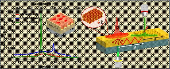
Researchers at the Indian Institute of Science (IISc), Bangalore, have have integrated two-dimensional (2D) semiconductor colloidal quantum wells (CQWs) with dielectric metasurface resonators (MSRs) to achieve unprecedented emission line narrowing and long- range photon transport at room temperature for on-chip photonic quantum information processing.
Led by Prof. Jaydeep K. Basu from IISc’s Department of Physics, in collaboration with Prof. Shankar Kumar Selvaraja from the Centre for Nano Science and Engineering (CeNSE), and theoretical support from Prof. Girish S. Agarwal at Texas A&M University, the study showcases the integration of Cadmium Selenide (CdSe)-based CQWs with a guided mode MSR. The MSR, fabricated on a silicon nitride (SiN) slab-waveguide platform, features a precise arrangement of holes in a square-lattice geometry. This design enables narrow resonances in both out-of-plane and in-plane directions, effectively tuning the light emission properties of CQWs.
The integration achieved remarkable results, including a 12-fold increase in brightness and a 97% reduction in the width of the emitted light’s spectral line, ensuring unparalleled spectral purity. The enhancement was enabled by the spectral overlap between the MSR’s narrow-band response and the broader emission from CQWs. The platform also demonstrated long-range photon transport across the chip, up to 1 mm, showcasing its potential for creating compact and efficient quantum devices.
“Our work shows how nanoscale materials like CQWs can be seamlessly integrated with photonic structures to achieve exceptional control over light emission and transport, which is critical for the next generation of quantum devices,” said Prof. Basu.
The researchers employed a state-of-the-art confocal setup for photoluminescence (PL) measurements, funded by the DST-FIST program, to study enhanced light properties with high precision. The findings have been published in the prestigious journal Advanced Optical Materials.
Looking ahead, the researchers aim to extend this platform to integrate single quantum emitters (SPEs) with MSRs to create highly efficient single-photon sources which are essential for quantum cryptography and quantum information processing.
Combining the spectral filtering capabilities of MSRs with the precise light emission of SPEs could unlock new possibilities in on-chip quantum photonics, enabling secure communications and advanced sensing technologies.

Fig1: Emission spectrum collected from confocal PL microscope funded by DST FIST.
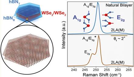
Figure caption: Left panel – schematic of twisted WSe2. Right panel – Raman spectra from natural and twisted bilayer of WSe2.


