A Major Push in Budget 2026 towards Semiconductor Self-Reliance
Introduction
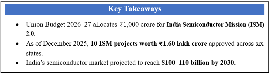
The Union Budget 2026–27 marked a decisive moment for India’s technology ambitions with the announcement of India Semiconductor Mission 2.0. The new phase signals a clear policy push to deepen domestic semiconductor capabilities at a time when chips underpin every critical digital and industrial system. ISM 2.0 will focus on producing semiconductor equipment and materials in India, designing full stack Indian semiconductor intellectual property, and fortifying both domestic and global supply chains. A provision of Rs. 1,000 crore has been made for ISM 2.0 for FY 2026–27, with a strong emphasis on industry led research and training centres to drive technology development and create a future ready skilled workforce.
Semiconductors are the backbone of modern electronics, powering computers, mobile devices, telecommunications, automobiles, defence systems and artificial intelligence. India has made steady progress in consolidating earlier investments into a full-stack value chain of its semiconductor ecosystem under ISM 1.0, expanding design capabilities and advancing fabrication, assembly and testing infrastructure across the country. This momentum reflects the broader vision of Aatmanirbhar Bharat and India’s transition from policy formulation to production readiness. Building on these gains, ISM 2.0 seeks to consolidate India’s position as a reliable and competitive participant in the global semiconductor network.
Sectoral Outlook: India’s Semiconductor Ecosystem
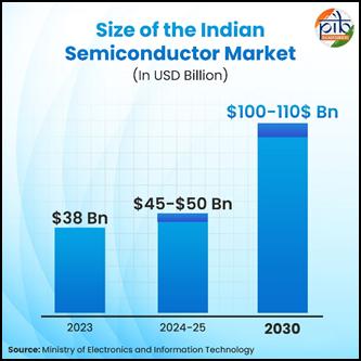
India is steadily emerging as a global semiconductor hub. Large scale investments, expanding manufacturing capacity, and platforms such as SEMICON India 2025 reflect growing global confidence in India’s semiconductor journey. The domestic chip market is witnessing rapid growth. As per industry estimates, the size of the Indian semiconductor market was about $38 Bn in 2023, $45-$50 billion in 2024-2025 and is expected to reach $100-$110 Bn by 2030. This expansion is anchored in the national vision of Make in India and Make for the World, positioning India as both a manufacturing base and a global supplier.
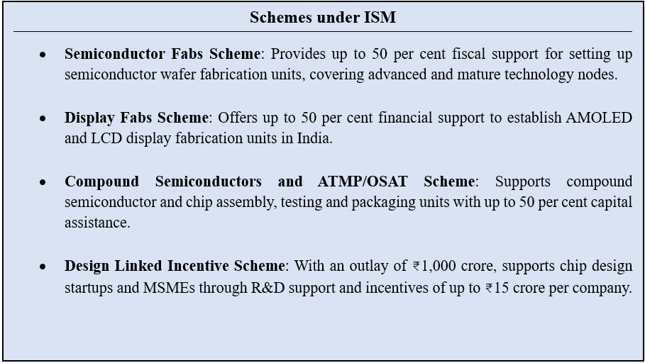
The foundation of this growth was laid with the approval of India Semiconductor Mission 1.0 by the Union Cabinet in December 2021. The Mission is supported by an incentive framework of ₹76,000 crore, offering fiscal support of up to 50 per cent for silicon fabs, compound semiconductor facilities, assembly and testing units, and chip design. As of December 2025, 10 projects with a total investment of ₹1.60 lakh crore have been approved across 6 states. These include silicon fabrication units, silicon carbide fabs, advanced and memory packaging facilities, and specialised assembly and testing infrastructure. Together, they are shaping a resilient domestic semiconductor ecosystem.
By 2029, India is expected to achieve the capability to design and manufacture chips required for nearly 70–75 per cent of domestic applications. Advancing on this foundation, the next phase under Semicon 2.0 will focus on advanced manufacturing, with a clearly defined roadmap to achieve 3-nanometre and 2-nanometre technology nodes. By 2035, India aims to be among the top semiconductor nations globally.
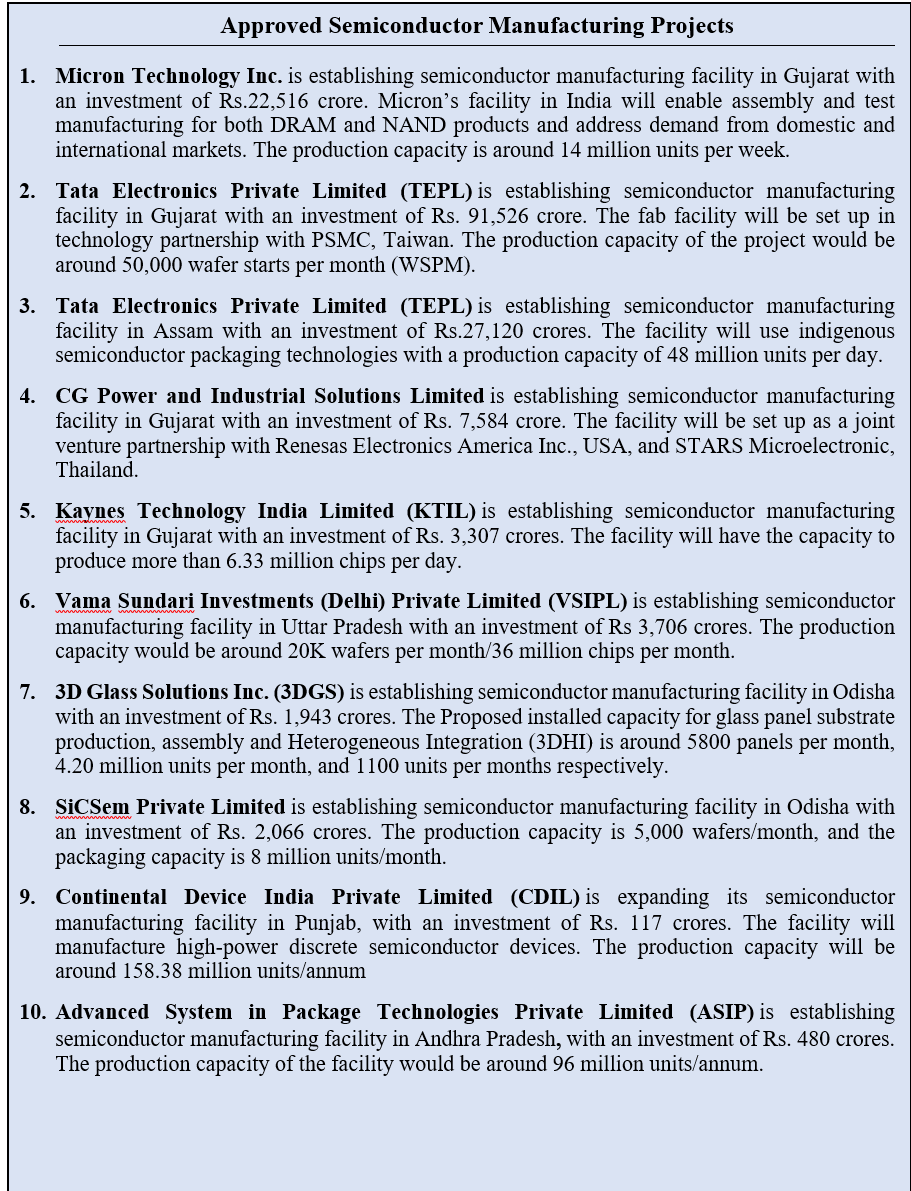
These facilities are expected to meet the growing chip requirements of key sectors such as consumer appliances, industrial electronics, automobiles, telecommunications, aerospace, and power electronics. Notably, several approved proposals are leveraging indigenous technologies for the assembly, testing, and packaging of semiconductor chips. This shift reflects India’s move towards deeper technological capability and reduced dependence on external systems, strengthening its position in the global semiconductor value chain.
Anticipated Impact of Semiconductor Programme in 2026–27
India’s semiconductor programme has been recalibrated in response to intensifying global competition and the concentration of advanced chip technologies among a limited number of players. Several countries with established semiconductor ecosystems are offering aggressive incentives, making it necessary for India to refine its approach. The modified programme therefore focuses on strengthening financial support for investments across semiconductor manufacturing, display fabrication, and the design ecosystem.
For 2026–27, the Modified Programme for Development of Semiconductor and Display Manufacturing Ecosystem in India has a total financial outlay of ₹8,000 crore. The programme aims to accelerate capital investment, generate high quality employment, and expand domestic capabilities across fabrication, packaging, and chip design. The projected outcomes for the year are outlined below.
Projected Targets under ISM for 2026–27:
| Scheme | Key Indicator | Projected Target |
| Modified Scheme for Semiconductor Fabs (Fabs to be Supported – 1) | Investment during the year | ₹4,000 crore |
| Employment generated | 1,500 persons | |
| Modified Scheme for Compound Semiconductors, Silicon Photonics, Sensors, Discrete Fabs and Assembly, Testing, Marking, and Packaging(ATMP)/ Outsourced Semiconductor Assembly and Test (OSAT) (Units to be Supported – 9) | Investment by units during the year | ₹11,000 crore |
| Employment generated by supported units | 3,000 persons | |
| Design Linked Incentive Scheme (Design companies to be supported – 30) | Semiconductor IP cores to be developed | 10 |
| Semiconductor design manpower employed | 200 persons |
Together, these outcomes reflect a strong push towards scaling domestic manufacturing, deepening design capabilities, and creating a skilled workforce to support India’s long term semiconductor ambitions.
Why the India Semiconductor Mission Matters
Semiconductors have become critical to the functioning of modern economies. Though rarely visible in everyday life, microprocessors quietly power systems that keep societies running. As highlighted in theEconomic Survey 2025–26, they form the backbone of energy networks, financial markets and telecommunications. They enable manufacturing units, hospitals, transport systems and satellites. A reliable supply of semiconductors is therefore essential for economic stability and continuity across sectors.
Recent global disruptions have underscored this dependence. The COVID-19 pandemic exposed serious weaknesses in semiconductor supply chains, with shortages affecting more than 169 industries worldwide. Production delays and rising costs followed, slowing economic activity across countries. These shocks revealed the risks of relying on a narrow set of suppliers. Today, the semiconductor industry is dominated by a few countries, including Taiwan, South Korea, Japan, China and the United States. Taiwan alone produces over 60 per cent of the world’s semiconductors and nearly 90 per cent of the most advanced chips, leaving global supply chains vulnerable to external shocks and geopolitical tensions.
In response, major economies are recalibrating their strategies. The United States, the European Union, Japan and South Korea have launched national initiatives to strengthen domestic chip manufacturing and diversify supply chains. India is positioning itself within this global shift as a trusted and reliable partner. The India Semiconductor Mission responds directly to this moment. By building domestic capacity across design, manufacturing and innovation, ISM represents a critical step towards self-sufficiency and technological sovereignty, while strengthening India’s role in a more resilient global semiconductor ecosystem.
At the core of this strategy lies a strong focus on semiconductor design and talent development, which together form the foundation of technological self-reliance.
Strengthening India’s Semiconductor Design Ecosystem
Since its launch in December 2021, the Design Linked Incentive Scheme has played a pivotal role in transitioning from capacity creation to technological depth in India. The scheme focuses on nurturing domestic innovation, supporting early-stage companies, and creating the foundation for a vibrant fabless ecosystem. It has also helped bridge the gap between academic research and industry application, strengthening India’s position in the global design landscape.
Key Achievements under the DLI Scheme (as of January 2026):
- The programme currently supports 24 semiconductor design startups across the country.
- Startups under the scheme have attracted nearly ₹430 crore in venture capital funding, reflecting growing investor confidence in India’s design ecosystem.
- Advanced Electronic Design Automation (EDA), the national chip design platform, has enabled access to high end design tools, with approximately 2.25 crore tool hours recorded.
- Around 67,000 students and over 1,000 start up engineers are actively using these tools for chip design and development.
- In academia, 122 designs have been taped out, with 56 chips fabricated at 180 nm at the Semiconductor Laboratory in Mohali.
- Startups have completed 16 tape outs, resulting in six chips fabricated at advanced foundry nodes, including technologies as advanced as 12 nm.
- Academic institutions have filed 75 patents, while startups have filed 10 patents, indicating a growing culture of innovation and intellectual property creation.
Looking ahead, the programme is set to scale further, with a target of enabling at least 50 fabless semiconductor companies in the next phase, reinforcing India’s ambition to emerge as a global hub for semiconductor design and innovation.
Advancing Indigenous Microprocessors and Core Semiconductor Technologies
Microprocessors form the foundational layer of modern digital infrastructure, powering devices and systems across telecommunications, mobility, healthcare, industry, defence, and space. Recognising their strategic importance, India has made focused investments to build sovereign capabilities in advanced processor design as a core pillar of semiconductor self-reliance.
A key milestone in this journey is the launch of DHRUV64, a fully indigenous 64-bit microprocessor developed by C-DAC under the Microprocessor Development Programme (MDP). Built on modern architectural principles, DHRUV64 delivers improved efficiency, multitasking capability, and reliability, enabling its deployment across sectors such as 5G infrastructure, automotive electronics, industrial automation, consumer devices, and the Internet of Things (IoT). Its development provides India with a secure, homegrown processor platform, reducing long-term dependence on imported chips—particularly significant given that India consumes nearly 20 per cent of global microprocessor output.
DHRUV64 builds on a growing portfolio of indigenous processors, including SHAKTI, AJIT, VIKRAM, and THEJAS, collectively forming the foundation of an Indian processor ecosystem. Developed under the Digital India RISC-V (DIR-V) Programme, these processors leverage the open-source RISC-V architecture, eliminating licence costs and enabling collaborative innovation across academia, startups, and industry. The rollout of DHRUV64, alongside the ongoing development of DHANUSH and DHANUSH+ System on Chips variants, strengthens India’s R&D ecosystem, accelerates product prototyping, and expands opportunities for domestic design talent.
Together, these initiatives position microprocessors not merely as components, but as strategic enablers of India’s digital sovereignty—supporting innovation, securing critical infrastructure, and anchoring the country’s long-term ambitions in the global semiconductor value chain.
Development of Semiconductor Talent Pipeline
A strong semiconductor ecosystem depends as much on people as on infrastructure. India has therefore adopted a comprehensive approach to build a large, skilled and industry ready talent base across design, manufacturing and advanced packaging. The emphasis is on early exposure to chip technologies, practical training, and continuous upskilling aligned with evolving industry requirements.
- Chips to Start up Programme: The Chips to Start up programme enables access to the latest electronic design automation tools across 397 universities and startups. Using these tools, chip designers from more than 46 universities have designed and fabricated 56 chips at the Semiconductor Laboratory in Mohali.
- Academic Programmes under All India Council for Technical Education (AICTE): Specialised academic programmes have been introduced to integrate semiconductor education into mainstream engineering. These include a B Tech in Electronics Engineering with focus on VLSI design, a diploma in integrated circuit manufacturing, and a minor degree in Electronics Engineering covering VLSI design and technology. Together, these programmes aim to produce graduates equipped with industry relevant skills.
- SMART Lab at NIELIT Calicut: The Skilled Manpower Advanced Research and Training Lab at NIELIT Calicut supports large scale training in semiconductor technologies. The initiative targets one lakh engineers across the country, with more than 62,000 engineers already trained, significantly strengthening the national talent pool.
- Industry Partnership with Lam Research: A large-scale training programme in nanofabrication and process engineering is being implemented in partnership with Lam Research. The focus is on building specialised skills for (ATMP) and advanced packaging facilities. The programme aims to generate 60,000 trained professionals over the next ten years.
- FutureSkills PRIME Programme: FutureSkills PRIME is a joint initiative of MeitY and NASSCOM designed to position India as a global digital talent hub. It focuses on skilling, reskilling and upskilling in emerging technologies, including semiconductors. Courses are developed with industry inputs and delivered through an online portal that enables learners to access training anytime and earn recognised skill certificates aligned with their aspirations.
Together, these initiatives are creating a robust and future ready semiconductor workforce, positioning India to sustain long term growth across the full chip value chain.
Conclusion
India Semiconductor Mission 2.0 marks a decisive shift from ecosystem creation to ecosystem consolidation and global integration. By deepening support for manufacturing, design, and advanced skills, ISM 2.0 positions semiconductors as a strategic national capability—central to economic resilience, digital infrastructure, and technological sovereignty. The enhanced budgetary support in 2026–27 provides the momentum required to accelerate execution, crowd in private investment, and scale domestic capacity across the full semiconductor value chain.
Looking ahead, ISM 2.0 lays the foundation for India to emerge as a trusted hub for semiconductor design, manufacturing, and innovation. With a clear roadmap for advanced nodes, strong design incentives, and a growing talent pipeline, India is poised to progressively reduce external dependencies while contributing to more resilient global supply chains. The Mission thus anchors India’s long-term ambition to be among the world’s leading semiconductor nations in the coming decade.